Reducing EMI in High-Speed Display Links
A practical guide to reducing EMI in high-speed display links through return-path control, differential routing, connector design, shielding, and pre-compliance testing.
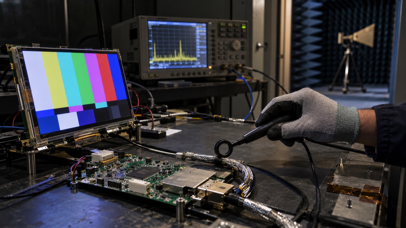
An embedded display can render a perfect image and still be the reason a product fails radiated-emissions testing. The panel, interface cable, controller, and enclosure form one electromagnetic system. A marginal return path at a connector or a centimeter of exposed cable shield can turn an otherwise balanced link into an efficient antenna.
The useful question is not simply, “Is LVDS low EMI?” It is: where can differential energy become common-mode current in this particular assembly? That question leads to fixes that survive cable changes, enclosure revisions, and volume production.
Why display links radiate
High-speed display interfaces move continuous or bursty data with fast edges. The fundamental pixel or lane frequency is only part of the problem. A sharp edge contains energy at many harmonics, often well above the clock named in the datasheet.
Differential signaling helps because equal and opposite currents ideally cancel their far fields. Real products are not ideal. Radiation increases when the pair sees:
- Unequal trace length or asymmetric via structures.
- Different parasitic capacitance on the two conductors.
- A split or void in the reference plane.
- Poor connector pin assignment or shield termination.
- An impedance step at a flex, adapter, or test point.
- Receiver imbalance or incorrect termination.
Texas Instruments’ LVDS SerDes layout guidance emphasizes solid reference planes, impedance continuity through connectors, avoiding board edges, and verifying transitions with time-domain reflectometry where appropriate. Those principles also apply to many other fast differential display links.
Find the current path before changing components
Every signal current returns to its source. At low frequency it tends to follow the path of least resistance; at high frequency it follows the path of least impedance, which normally means directly beneath the signal on its reference plane.
Draw the complete loop from transmitter to panel and back. Include:
- SoC or bridge IC escape routing.
- Every reference-plane transition.
- Common-mode choke or AC-coupling pads, if used.
- Board connector, cable, and panel connector.
- Cable shield and chassis connection.
- Panel ground pins and metal frame.
If a pair changes layer, place nearby ground stitching vias so return current can change reference planes without taking a long detour. If the pair crosses a plane split, reroute it. A stitching capacitor across two power reference areas may help in some architectures, but it is not a substitute for an uninterrupted ground reference.
Control the differential pair as one structure
“Length matched” does not guarantee a quiet link. The pair must remain coupled and geometrically balanced.
Maintain impedance through the whole channel
Set trace width, spacing, dielectric height, and copper thickness with the PCB fabricator. Then examine connector pads, layer changes, flex stack-up, and cable geometry. A 100-ohm differential PCB pair connected to an uncontrolled ribbon section is not a 100-ohm channel.
Use the impedance required by the transmitter, receiver, and interconnect specification. Do not copy a value from another interface. For an assembly with detachable wiring, the controlled-impedance display cable design matters as much as the main PCB.
Match within the pair, not between unrelated pairs
Intra-pair skew converts some differential signal into common mode. Keep the positive and negative conductors symmetric. Avoid long serpentine compensation on only one conductor; tightly folded meanders add crosstalk and local discontinuities.
Pair-to-pair matching requirements depend on the interface. Do not add unnecessary tuning simply to make every lane visually identical.
Avoid stubs and casual test points
An unpopulated connector, probe pad, or long via stub can create a resonant discontinuity. Provide a deliberate measurement strategy: compact probe footprints, removable series elements, or a dedicated characterization coupon. After validation, depopulate or isolate optional branches.
Connector and cable decisions often dominate
Many boards pass when tested without the final display cable and fail after mechanical integration. That is a strong sign that the interconnect or chassis coupling is involved.
For a shielded cable, aim for a short, low-inductance, preferably circumferential shield connection at the enclosure boundary. A long drain wire has much more high-frequency impedance than its DC resistance suggests. Whether the shield bonds at one end, both ends, or through a hybrid network depends on product grounding, safety, ESD, and frequency. Treat it as a system decision, not folklore.
For unshielded FPC, use adjacent grounds where the pin budget allows, preserve pair spacing through bends, and keep the flex away from enclosure seams, antennas, switching inductors, and unfiltered external cables. Document the routing and bend zones so production units match the passing prototype.
Termination, drive strength, and edge rate
More drive is not automatically more margin. Excessive swing or the fastest available slew rate can increase overshoot and high-frequency energy without improving the receiver eye.
Start with the transmitter and panel recommendations. Then validate:
- Differential amplitude at the receiver.
- Common-mode voltage and common-mode ripple.
- Rise/fall time.
- Overshoot, undershoot, and ringing.
- Receiver eye or error counters when available.
- Performance across voltage, temperature, and cable lots.
A common-mode choke can reduce common-mode noise, but it also adds differential insertion loss, mode conversion, and parasitics. Select it from measured noise and channel data, not because a reference schematic happens to include one.
Spread-spectrum clocking can lower narrow peaks by distributing energy, but only when both ends support the modulation and the chosen profile meets interface limits. It should refine a sound channel, not hide a broken return path. MIPI describes D-PHY as a clock-forwarded link with scalable data lanes, and the organization identifies low EMI as a core interface objective in its current specification portfolio.
Separate link emissions from power-converter noise
The display assembly usually contains at least three possible noise families:
| Suspect | Typical clue | Useful experiment |
|---|---|---|
| Pixel/lane link | Peaks move with resolution, refresh, or pattern | Change timing or display a low-transition test pattern |
| Backlight PWM | Peaks follow dimming frequency and harmonics | Hold brightness at 100% or use a temporary DC condition |
| DC/DC converter | Peaks track load or switching mode | Power from a quiet bench source, if safe |
| Cable common mode | Probe response is strongest along cable/shield | Re-route cable or add temporary ferrite for diagnosis |
| Enclosure seam | Hot spot at slot or connector aperture | Temporarily bridge seam with conductive tape |
Temporary ferrites, copper tape, and absorbers are diagnostic tools. If they change the result, they identify a coupling path. They are not automatically the best production fix.
Use test patterns as electrical stimuli
Different images create different switching activity. Test at least:
- All black and all white.
- Alternating one-pixel checkerboard.
- Vertical and horizontal stripes.
- Color bars.
- A realistic animated UI.
- Maximum supported resolution and refresh.
Record the exact timing mode and pattern beside each scan. A quiet static screen does not prove an interface is quiet in normal use. Calculate the expected pixel and serial rates first; this display bandwidth and lane-rate calculation helps predict where clock-related families may appear.
A practical pre-compliance sequence
- Establish a repeatable configuration, cable route, grounding state, brightness, and test image.
- Run a current-probe or near-field scan to locate hot structures.
- Correlate peaks with pixel clock, lane clock, PWM, and converter frequencies.
- Change one variable at a time.
- Save plots, photographs, firmware revision, and physical configuration.
- Recheck at temperature and with cable/panel samples from more than one lot.
- Confirm the final build in a calibrated chamber against the applicable standard.
Near-field probes do not predict regulatory field strength directly. They are excellent for comparison and localization when probe position and analyzer settings are controlled.
Design review checklist
- Differential impedance is defined for PCB, connector, cable, and flex.
- No high-speed pair crosses a reference-plane split.
- Layer transitions have an adjacent return-path via.
- Intra-pair geometry remains symmetric through pads and bends.
- Optional test branches do not create permanent stubs.
- Cable shield termination is short and mechanically repeatable.
- Display cable routing is controlled in the mechanical drawing.
- Backlight and power-converter noise are tested separately.
- Drive strength and slew rate use the lowest setting that retains margin.
- Pre-scan records include image pattern, mode, brightness, and software build.
For larger embedded systems, a stable 15.6-inch LVDS display platform can serve as a useful reference load while cable, controller, and enclosure changes are evaluated. The important point is to freeze the panel revision and all adapters while comparing EMI results.
Most display-link EMI problems are current-path problems. Begin with balance, reference continuity, and the final physical assembly. Add filtering only after measurement identifies the mode that needs treatment. A channel that is electrically clean, mechanically controlled, and documented is much more likely to pass again after the next supplier lot or enclosure revision.