Choosing a Display Bridge IC: HDMI, LVDS, eDP, and MIPI
Select a display bridge IC by protocol direction, timing, pixel clock, lane rate, color format, EDID, HDCP, scaling, power, software, PCB, and lifecycle needs.
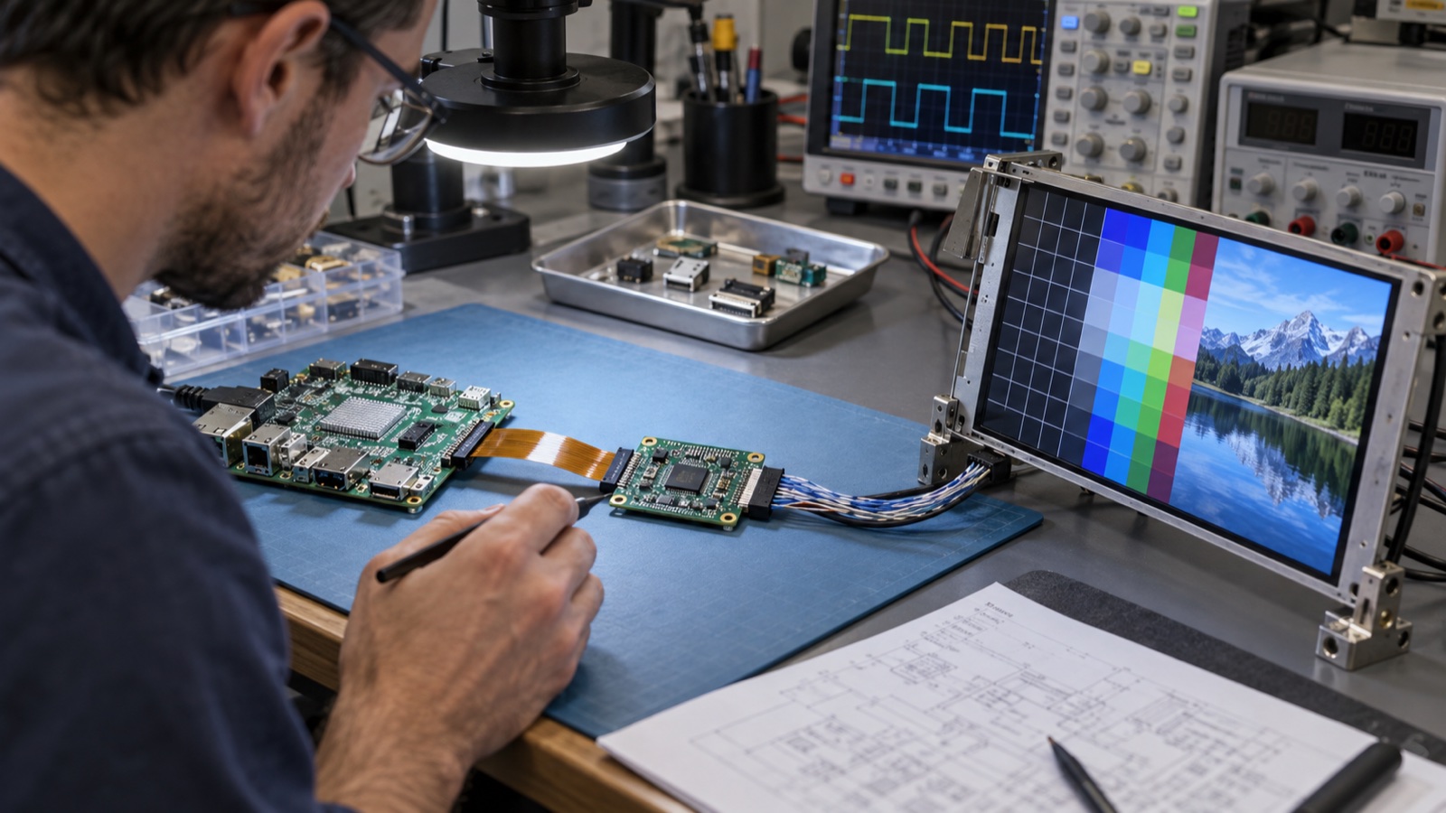
A display bridge IC is often introduced with a sentence such as “the processor has MIPI DSI, the panel has LVDS, so add a DSI-to-LVDS bridge.” That describes the protocol names but not whether the system will work.
The bridge must accept the source’s exact lane configuration and video format, generate the panel’s timing and electrical mapping, start in the correct order, fit the PCB channel, and remain available for the product lifecycle. It may also need EDID handling, HDCP, audio, scaling, frame buffering, test patterns, or automotive diagnostics.
Treat the bridge as a small display subsystem, not a passive adapter.
Direction is the first filter
Bridge direction is fixed. An HDMI-to-MIPI DSI device is not a MIPI DSI-to-HDMI transmitter. An RGB-to-LVDS serializer does not necessarily recover LVDS and output RGB.
Write the path explicitly:
source device -> source protocol -> bridge -> sink protocol -> display
Examples:
- SoC MIPI DSI host → DSI-to-LVDS bridge → single-link LVDS panel.
- HDMI input → HDMI receiver/DSI transmitter → MIPI DSI panel.
- Parallel RGB LCD controller → RGB-to-LVDS bridge → LVDS panel.
- DisplayPort source → eDP-compatible path → embedded panel.
Also identify whether each side is a transmitter, receiver, host, or peripheral. Product-page wording such as “supports HDMI and MIPI” is not enough.
Confirm the source before choosing the bridge
Record the source capabilities:
- Protocol and version.
- Number of lanes or parallel bus width.
- Minimum/maximum clock or lane rate.
- Video and command modes.
- Pixel formats and bit packing.
- Sync/DE behavior.
- Clock polarity and continuous/non-continuous mode.
- Available reference clocks.
- EDID, HPD, AUX, I²C, or control interfaces.
- Driver support in the operating system.
A DSI source may support four lanes physically but expose only two on the chosen package. A processor may support DSI video mode but not the command mode expected by the panel. An HDMI source may require EDID before it emits the desired resolution.
The processor-to-panel interface comparison provides the wider architectural context before a bridge is added.
Confirm the panel timing and mapping
From the exact panel specification, collect:
- Native active resolution.
- Horizontal and vertical totals and allowed ranges.
- Pixel-clock range.
- Refresh-rate range.
- Color depth and mapping.
- Interface link/lane count.
- Supply and I/O voltage.
- Reset, standby, and backlight timing.
- Connector pinout and cable requirements.
For LVDS, mapping details are critical. “24-bit LVDS” can still differ by JEIDA/VESA assignment, pair order, polarity, single/dual link, and odd/even pixel handling. A bridge that reaches the right pixel clock can produce swapped colors or a split image when mapping is wrong.
For a higher-resolution panel such as a 10.1-inch 1920×1200 IPS module, the bridge’s maximum pixel clock and input-lane rate should be checked with the exact blanking—not just the active resolution.
Build a bandwidth chain, not one number
Calculate each segment separately:
SoC output capability
    -> bridge input lane rate
    -> internal bridge pixel clock
    -> bridge output link rate
    -> panel accepted timing
The bridge can be limited by any of the following:
- Aggregate input bandwidth.
- Rate per input lane.
- Number of lanes.
- Internal pixel clock.
- Output serializer clock.
- Maximum resolution at a stated blanking mode.
- Supported bits per pixel.
- PLL input/reference frequency.
TI’s SN65DSI83, for example, is specified as a single-channel DSI-to-single-link LVDS bridge with up to four 1 Gbit/s D-PHY lanes, RGB666/RGB888 packets, and an LVDS output clock range of 25–154 MHz. Those values are more useful than the shorthand “supports WUXGA,” because they can be checked against the design.
Use the display bandwidth and lane-rate worksheet to retain the calculations with the bridge configuration.
Determine whether the bridge scales or only translates
Many bridge ICs translate protocol without resizing the image. If the source sends 1280×720 and the panel is 1280×800, the bridge may not create the missing lines or reposition the image.
Check explicitly for:
- Horizontal/vertical scaling.
- Cropping and windowing.
- Color-space conversion.
- Frame-rate conversion.
- Rotation.
- Deinterlacing.
- Frame buffering.
These functions require memory and add cost, latency, power, and configuration complexity. A simple line buffer only absorbs short-term rate differences; it does not provide arbitrary scaling.
If the system can make the SoC output native panel timing, a protocol-only bridge is simpler. If the source mode is fixed, a scaler or FPGA may be required.
HDMI adds EDID, HPD, audio, and possibly HDCP
HDMI is more than a pixel stream. A receiver or transmitter design may need:
- Hot-plug-detect behavior.
- EDID storage and mode advertisement.
- TMDS rate support.
- Color format and quantization range.
- Audio extraction or insertion.
- HDCP licensing, keys, and version support.
- CEC if the product requires it.
- ESD protection for an external connector.
If HDMI exists only as an internal board-to-board link, ask whether it is still the lowest-risk choice. MIPI DSI, LVDS, or eDP may better match the panel, while HDMI can remain at an external input boundary.
Never claim protected-content compatibility solely because the bridge data sheet mentions HDCP. The whole product needs the correct licenses, keys, security path, and source/sink behavior.
eDP and DisplayPort require link management
An eDP path uses AUX communication, link training, defined link rates/lane counts, and panel power timing. A protocol converter must coordinate those functions; it cannot simply forward pixel clock.
Check:
- Supported DisplayPort/eDP version and link rates.
- Number of lanes.
- AUX and HPD implementation.
- Link-training control.
- EDID or DisplayID handling.
- Backlight control and panel power sequence.
- Adaptive-sync, PSR, DSC, or other optional features if required.
VESA describes eDP as a standardized embedded panel interface derived from DisplayPort and designed to increase resolution, color depth, refresh capability, and system integration. Optional features should be treated as optional until both bridge and panel prove support.
Software support can outweigh hardware elegance
A bridge can be electrically perfect and still delay a project because its register programming is undocumented or unsupported on the target OS.
Review:
- Public data sheet and programming guide availability.
- Linux DRM/bridge driver or vendor BSP support.
- Device-tree bindings.
- Firmware update process.
- Reference register scripts.
- Vendor configuration tools.
- Access to application support.
- Error/status registers and test patterns.
Confirm whether the driver supports the exact topology and kernel/BSP version. “There is a Linux driver” may refer to a different input, output, or board.
For bare-metal systems, obtain a complete initialization sequence and understand every clock/timing value. A large undocumented binary table is a lifecycle risk.
Clock architecture deserves its own review
The bridge may derive output timing from:
- Recovered input clock.
- Continuous DSI clock.
- External crystal or oscillator.
- SoC reference clock.
- Internal PLL with restricted ratios.
Clock decisions affect jitter, allowable modes, sleep behavior, startup, and EMI. Verify reference accuracy and availability before bridge reset release. Check whether the bridge can lock across panel timing tolerances and temperature.
If the input disappears, define the output behavior. The bridge should not leave the panel clocking random pixels with the backlight on.
Power, reset, and backlight must form one sequence
Bridge rails, panel rail, source interface, reset, link training, valid video, and backlight enable must be coordinated. The LCD rail and backlight sequencing procedure should include bridge PLL lock and output enable.
Test cases should include:
- Source boots before bridge.
- Bridge boots before source.
- Panel is reset while bridge remains powered.
- Source changes mode.
- Cable is absent or poorly connected.
- Brownout affects only one rail.
- Sleep/resume repeats rapidly.
Some bridges can output a test pattern before the source is ready. This is useful for isolating the output side, but production firmware should not leave test mode accessible accidentally.
PCB implementation is part of the bridge choice
The bridge sits between two signal-integrity problems. Package and pinout can make or break routing.
Review:
- BGA escape and PCB layer count.
- Pair impedance and spacing.
- Lane/pair swap capability.
- Intra-pair and inter-pair skew.
- Reference-plane continuity.
- Return-current path through connectors.
- Location of termination and AC coupling.
- Reference-clock isolation.
- Power filtering and decoupling.
- Thermal pad and junction temperature.
A lane-swap feature can reduce vias; it cannot fix every protocol’s logical lane ordering. Confirm what the device allows before the layout uses it.
Latency is usually small—until scaling or buffering appears
Pure protocol bridges may add only line-scale latency. Scalers and frame-rate converters can add one or more frames. Camera, control, and touch-feedback applications may notice that delay.
Measure end-to-end latency with the final configuration. Do not rely on a generic “low latency” statement when the selected mode enables buffering.
Lifecycle and qualification are first-class requirements
Bridge ICs can become the hardest component to replace because they touch hardware, software, timing, and compliance simultaneously.
Ask:
- Is the device active and recommended for new designs?
- Is an automotive or industrial temperature grade required?
- Are PCN and EOL notifications available?
- Is there a pin-compatible alternative?
- Can the panel or SoC be changed to remove the bridge in a future revision?
- Are evaluation boards and configuration tools still supported?
- Does the supplier provide IBIS models and layout guidance?
Qualify more than one production lot if the application is sensitive to PLL, link, or thermal behavior.
Bridge selection worksheet
| Category | Evidence required |
|---|---|
| Direction | Exact input receiver and output transmitter |
| Video | Native resolution, totals, refresh, bpp |
| Input | Lanes, rates, modes, clock behavior |
| Output | Link mapping, rates, voltage, termination |
| Processing | Scaling, buffering, conversion, latency |
| Control | I²C/SPI, EDID, AUX, HPD, interrupts |
| Software | Driver, register tool, error diagnostics |
| Power | Rails, reset, lock, sleep, shutdown |
| PCB | Package, impedance, swap, reference planes |
| Compliance | HDMI/HDCP or protocol obligations |
| Reliability | Temperature, qualification, lifecycle |
Prototype with an evaluation module—but do not stop there
An evaluation module proves that the chip can operate in a friendly setup. It may use short cables, an ideal oscillator, carefully filtered supplies, and vendor scripts.
After initial proof:
- Recreate the exact panel timing.
- Use the production source and BSP.
- Move to production cable length and connector.
- Test boot-order variations and error recovery.
- Run temperature and voltage corners.
- Scan EMI with worst-case image traffic.
- Log bridge status over long-duration cycling.
For a larger LVDS/eDP module such as a 15.6-inch high-brightness display, cable and link margin should be verified in the final enclosure rather than inferred from an open-bench evaluation board.
FAQ
Can any MIPI DSI bridge drive any DSI source?
No. Lane count, lane rate, D-PHY version, clock mode, packet format, video/command mode, and software must match.
Does a DSI-to-LVDS bridge change resolution?
Many do not. They translate transport while preserving the pixel stream. Scaling must be explicitly listed.
Is an FPGA a better display bridge?
It can provide custom timing, scaling, and diagnostics, but adds development, power, cost, configuration, and lifecycle work. Use it when fixed-function bridges cannot satisfy the requirements.
Should a bridge IC be placed near the processor or panel?
Placement depends on which interface tolerates the longer channel, routing constraints, power, and EMI. Analyze both sides rather than using a universal rule.
Technical references
- TI SN65DSI83 product documentation — a concrete DSI-to-LVDS example with lane, format, pixel-clock, and temperature limits.
- Toshiba HDMI-to-MIPI bridge documentation — illustrates the opposite protocol direction and higher-bandwidth HDMI receiver use case.
- VESA eDP overview — official context for embedded DisplayPort performance and integration.