How to Calculate Display Interface Bandwidth and Lane Count
Calculate pixel clock, active video payload, blanking, link overhead, LVDS rate, and MIPI DSI lane count with worked embedded-display examples and margin rules.
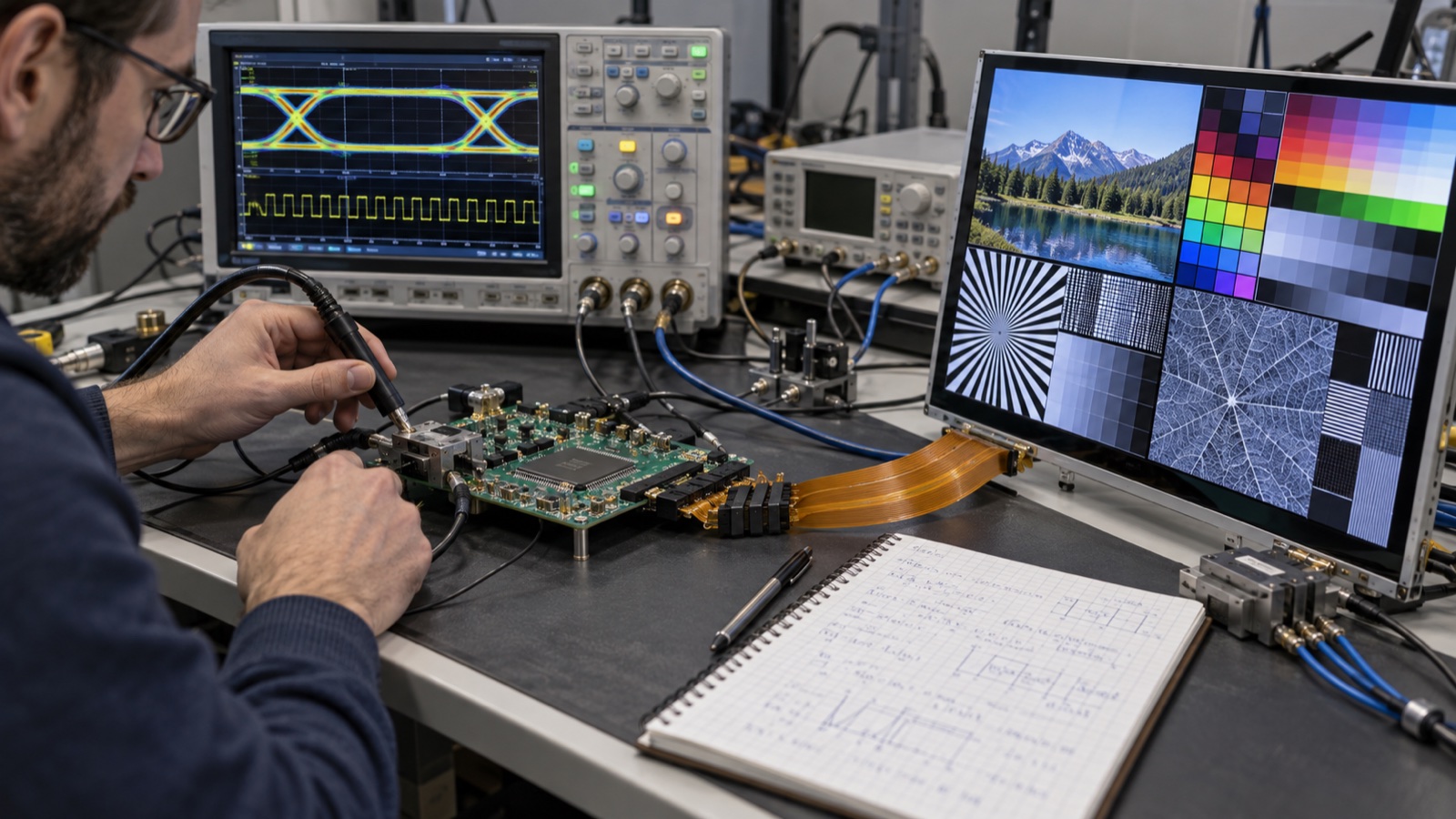
Display bandwidth calculations often begin with width × height × frame rate × bits per pixel. That product is useful, but it is only the active-image payload. Real links also carry blanking intervals, packet headers, synchronization, line overhead, encoding, and implementation margin.
A design can pass the simple calculation and still fail because the host cannot generate the panel’s exact timing, the bridge IC has a lower pixel-clock limit, or the chosen MIPI DSI lane rate leaves no room for protocol overhead.
The safest process is to calculate the raster first, translate it into the rules of the selected interface, and then verify every device in the path.
Collect the panel timing before calculating anything
Use the timing table for the exact panel revision. Record:
- Horizontal active pixels (
Hactive). - Horizontal front porch, sync width, and back porch.
- Vertical active lines (
Vactive). - Vertical front porch, sync width, and back porch.
- Refresh rate.
- Pixel clock minimum, typical, and maximum.
- Pixel format or color depth.
- Interface mode, mapping, and lane count.
The totals are:
Htotal = Hactive + Hfront + Hsync + Hback
Vtotal = Vactive + Vfront + Vsync + Vback
Nominal pixel clock is:
pixel clock = Htotal × Vtotal × refresh rate
If the datasheet already provides a pixel-clock range, treat it as authoritative. Recalculate it to catch transcription errors and understand where the number comes from.
Active payload is a lower bound
The active image payload is:
active payload = Hactive × Vactive × refresh rate × bits per pixel
For 1280×800 at 60 Hz and RGB888:
1280 × 800 × 60 × 24 = 1.475 Gbit/s
That number excludes blanking and link protocol. If total timing is 1440×823, the raster pixel clock is:
1440 × 823 × 60 ≈ 71.1 MHz
A 24-bit stream across the whole raster represents:
71.1 million pixels/s × 24 bits ≈ 1.706 Gbit/s
The difference between 1.475 and 1.706 Gbit/s is not wasted arithmetic. It is timing space the interface and panel may require.
Bits per pixel must match the actual transport
Common uncompressed RGB formats include:
| Format | Transport depth |
|---|---|
| RGB565 | 16 bits/pixel |
| RGB666 packed | 18 bits/pixel |
| RGB666 loosely packed | Often transported in 24-bit units |
| RGB888 | 24 bits/pixel |
| RGB101010 | 30 bits/pixel |
Do not infer transport depth from what the framebuffer API calls the image. A system can render RGB565, expand to RGB888 at the display controller, and then send 24 bits per pixel. Conversely, some interfaces pack 18-bit data efficiently while others use wider containers.
The display color-depth and pipeline review helps separate panel depth, framebuffer format, and link format.
Pixel clock is the key number for parallel RGB
Parallel RGB transfers one pixel per clock across 16, 18, or 24 data wires. The required clock comes from total horizontal and vertical timing, not active resolution alone.
Check:
- Host LCD-controller maximum clock.
- Setup and hold time at the panel connector.
- Clock polarity and data-sampling edge.
- Data-enable versus sync mode.
- Signal-voltage compatibility.
- PCB and cable skew.
- Memory bandwidth to sustain every pixel.
An MCU may list a 90 MHz LCD controller but still be unable to feed it continuously when SDRAM, CPU, and graphics accelerator share the same bus. Measure under the actual render workload.
LVDS converts pixel clock into serialized pair rate
Many single-link TFT LVDS interfaces use four data pairs plus a clock pair. A common mapping serializes seven bits on each data pair for every pixel clock:
LVDS serial bit rate per data pair ≈ pixel clock × 7
At a 71.1 MHz pixel clock:
71.1 MHz × 7 ≈ 497.7 Mbit/s per data pair
The mapping may be JEIDA or VESA, and the number of links can change at higher pixel clocks. Confirm:
- Single-link or dual-link.
- 18-bit or 24-bit mapping.
- JEIDA/VESA bit assignment.
- Odd/even pixel distribution for dual link.
- Allowed LVDS clock range.
- Clock and data polarity options.
Bandwidth is necessary but not sufficient. A bridge with enough aggregate throughput can still fail if its supported pixel-clock range or mapping does not match the panel.
MIPI DSI lane count needs protocol margin
For a first-pass DSI estimate:
minimum payload rate per lane = active payload / number of lanes
A more conservative video-mode estimate uses the full raster:
estimated lane rate = pixel clock × transported bits per pixel
                      / number of lanes
                      × overhead factor
The overhead factor depends on video mode, packet structure, blanking treatment, low-power intervals, burst behavior, and host implementation. A 5–15% planning allowance can be useful early in architecture, but it is not a substitute for the host vendor’s DSI calculation tool or timing requirements.
Using the 1280×800 example with RGB888, two lanes, and a provisional 10% allowance:
1.706 Gbit/s / 2 × 1.10 ≈ 0.938 Gbit/s per lane
If the host and panel are each limited to 1.0 Gbit/s per lane, this is technically close and operationally uncomfortable. Four lanes reduce the rate to roughly 469 Mbit/s per lane and create more margin, but consume additional pins and routing.
Worked example: 1920×1200 at 60 Hz
Assume illustrative total timing of 2080×1235 at 60 Hz, RGB888:
pixel clock = 2080 × 1235 × 60
            ≈ 154.1 MHz

full-raster bit rate = 154.1 MHz × 24
                     ≈ 3.699 Gbit/s
For four DSI lanes with a provisional 10% margin:
3.699 / 4 × 1.10 ≈ 1.017 Gbit/s per lane
This result immediately creates review questions:
- Does the host support four lanes above 1.02 Gbit/s?
- Does the panel accept that lane rate and selected clock mode?
- Does the bridge, if present, support a 154 MHz pixel clock?
- Are the assumed porches valid for the exact module?
- Can reduced blanking be used?
- Does the PCB stack and connector support the required channel?
The 10.1-inch 1920×1200 panel format shows why resolution alone cannot select a host. Native timing and interface implementation close the calculation.
DSI video modes change how blanking is carried
Non-burst video with sync pulses, non-burst with sync events, and burst mode do not use the high-speed link identically. Some blanking can be represented with packets or low-power time rather than transmitting 24-bit blank pixels continuously.
Therefore, pixel clock × bpp is a conservative architecture number, not always the exact wire rate. The host controller may impose minimum lane speed, byte-clock relationships, packet-size restrictions, or limits on low-power entry between lines.
Use the silicon vendor’s tool or register model after the first-pass calculation. Save its inputs and output with the design record so firmware and hardware teams are using the same assumptions.
Command mode is traffic-dependent
DSI command mode can update selected regions instead of streaming every raster continuously. Average traffic can be far lower for a static UI. Peak traffic still matters when a large region changes.
Estimate:
update payload = changed pixels × bits per pixel × updates per second
Then include command packets, address-window commands, line boundaries, acknowledgments if used, and bus efficiency. Also check whether the panel has enough memory and how tearing-effect synchronization limits the update window.
The architectural comparison of SPI, RGB, and MIPI DSI update behavior is useful before deciding that average bandwidth alone makes command mode the best choice.
eDP and DisplayPort add link encoding and lane rates
DisplayPort-family links use defined lane rates and coding schemes rather than an arbitrary bit rate. Usable video payload is lower than raw aggregate lane rate because of line coding and transport overhead.
The calculation process is:
- Determine uncompressed video payload from timing and format.
- Account for the applicable coding efficiency and transport overhead.
- Select a supported lane rate and lane count on both source and sink.
- Verify link training, AUX support, and panel power sequence.
- Add audio or other payload only where relevant.
Do not mix eDP version labels, DisplayPort link rates, and panel capability. The source, cable, connector, and panel must share a valid combination.
Compression is an architecture choice, not free bandwidth
VESA Display Stream Compression (DSC) can reduce link traffic while maintaining visually lossless quality. MIPI DSI and eDP ecosystems can incorporate DSC, but both ends need compatible versions and parameters.
Compression adds questions about:
- Slice dimensions.
- Bits per pixel after compression.
- Encoder availability in the source.
- Decoder support in the panel or bridge.
- Buffering and latency.
- Error behavior.
- Firmware configuration and interoperability.
Do not use a nominal 3:1 compression ratio to rescue an unsupported architecture unless the complete chain is specified and tested.
Memory bandwidth can exceed link bandwidth
The display link reads the final frame. The renderer may read backgrounds, icons, fonts, and prior layers, then write intermediate and final buffers. Rotation and scaling add more traffic.
A simplified estimate might include:
- Final scanout read.
- Render target write.
- Texture and source-layer reads.
- Double/triple buffer operations.
- Video decode output.
- CPU or DMA access sharing the same memory.
A link requiring 1.7 Gbit/s can coexist with several times that amount inside memory. Use performance counters or measured worst-case scenes rather than assuming link payload equals total system bandwidth.
Add margin in the right place
Margin should not mean arbitrarily increasing clocks. Use it to ensure the selected standard operating point is comfortably inside device limits.
Check margin for:
- Pixel-clock tolerance.
- Lane-rate ceiling and floor.
- Oscillator accuracy.
- Temperature and voltage.
- Cable/connector loss and skew.
- Memory contention.
- Firmware latency and underrun risk.
- Alternate panel timing.
If success requires maximum host lane rate, minimum blanking, best-case oscillator, and no graphics contention, the architecture has no real margin.
A calculation worksheet for design reviews
Record the following in one controlled sheet:
| Input | Value/source |
|---|---|
| Panel part and revision | Exact specification |
| Active resolution | H × V |
| H/V porch and sync | Min/typ/max |
| Refresh rate | Required range |
| Pixel clock | Calculated and datasheet |
| Transport format | RGB565/666/888/etc. |
| Interface mode | RGB, LVDS, DSI mode, eDP |
| Lane count/rate | Supported combination |
| Protocol assumptions | Coding, packet, blanking, DSC |
| Host limit | Datasheet and clock tree |
| Bridge limit | Pixel and link clocks |
| Measured margin | Prototype evidence |
The TFT timing table review process helps locate the source values and separate typical timing from allowed ranges.
Verify calculation with hardware
On a prototype:
- Measure pixel clock and relevant sync timing.
- Read DSI/bridge status and error counters where available.
- Test solid colors, checkerboards, gradients, video, and heavy GUI scenes.
- Run memory stress and peripheral traffic concurrently.
- Test min/max voltage and temperature.
- Use the production cable and connector.
- Repeat boot, sleep, resume, and hot-plug behavior where applicable.
Bandwidth problems often appear as intermittent line shifts, blank frames, colored sparkles, underruns, or failures only during animation. A static logo is a weak test.
FAQ
Is width × height × refresh × bpp enough?
It gives active payload. Include blanking, protocol/coding overhead, and device-specific constraints before choosing a link.
How much margin should a DSI lane calculation use?
Use the host vendor’s exact method. During early planning, 5–15% may expose marginal choices, but DSI mode and implementation determine the real requirement.
Does reduced blanking always work with an LCD panel?
No. The exact panel timing table defines acceptable porches, sync widths, and pixel-clock range. Do not import timing from another module.
Can DSC reduce the required lane count?
Yes when source, transport, bridge, and sink all support compatible DSC parameters. It cannot be assumed from a standard name alone.
Technical references
- MIPI Alliance DSI specification overview — official description of DSI architecture, D-PHY use, video capability, and reduced pin count.
- VESA Display Stream Compression overview — explains DSC integration with embedded display interfaces and its low-latency, visually lossless goal.
- VESA embedded DisplayPort overview — discusses higher link performance, color depth, resolution, and DSC in eDP.